Semiconductor Packaging Metrology News: Key Shifts in 2026
Time
Click Count
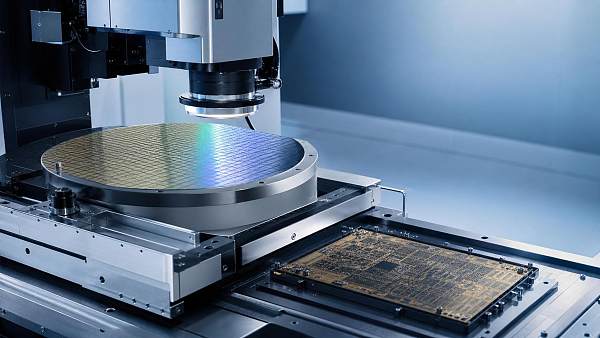
In 2026, metrology in semiconductor packaging news is increasingly defined by narrow tolerances, hybrid architectures, and zero-defect expectations. The most meaningful shift is not inspection speed alone. It is the growing role of measurement intelligence in yield control, supplier qualification, process traceability, and capital planning across advanced packaging environments.
Across the broader industrial landscape, semiconductor packaging now influences electronics, automotive systems, aerospace modules, medical devices, and communications infrastructure. That makes metrology in semiconductor packaging news relevant beyond fabs. It now affects reliability models, sourcing strategies, compliance preparation, and roadmap timing in adjacent precision industries.
Why 2026 news matters differently across packaging scenarios
Not every packaging line faces the same risk profile. A fan-out package, a 2.5D interposer, and a power module require different measurement priorities. Reading metrology in semiconductor packaging news without scenario context can lead to wrong equipment assumptions and weak benchmarking decisions.
In 2026, three forces are driving this divergence. First, heterogeneous integration increases layer interaction complexity. Second, warpage sensitivity rises as package sizes grow. Third, data-linked verification becomes mandatory for tighter customer audits and regulatory expectations.
This means advanced measurement must be judged by use case. Optical topography may solve one bottleneck. X-ray reconstruction may solve another. In other cases, electrical test correlation determines whether metrology investment creates measurable process value.
Scenario 1: Heterogeneous integration lines need cross-domain verification
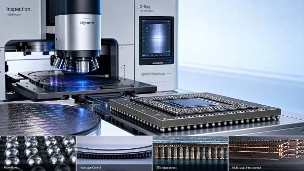
The strongest theme in metrology in semiconductor packaging news is heterogeneous integration. Chiplets, interposers, wafer-level redistribution, and advanced substrates are increasing inspection complexity at every interface.
In this scenario, single-point measurement is no longer enough. Dimensional metrology, optical inspection, and defect review must connect to one decision flow. The key judgment point is correlation between geometric accuracy and final electrical behavior.
Core judgment points
- Can bump height, coplanarity, and overlay be measured on the same data backbone?
- Does the toolset support sub-micron alignment verification across mixed materials?
- Is measurement output linked to electrical failure analysis or only visual pass-fail review?
- Can the workflow detect process drift before assembly scrap rises?
Where these links are weak, inspection may look modern but still miss root causes. That is why metrology in semiconductor packaging news increasingly highlights unified analytics, not standalone sensors.
Scenario 2: High-volume packaging lines focus on cycle time with trusted accuracy
For high-volume consumer and computing packages, throughput remains critical. Yet 2026 reporting shows a shift. Faster measurement is valuable only when uncertainty, repeatability, and false-call rates stay under control.
This scenario often uses optical inspection, non-contact profilometry, and AI-assisted defect classification. The practical question is whether automation reduces escapes without increasing unnecessary holds. That is a central theme in metrology in semiconductor packaging news.
Core judgment points
- Measurement speed must match takt time without hidden sampling compromises.
- AI defect models need periodic retraining against verified reference datasets.
- Gauge capability must remain stable across shift changes and substrate variations.
- Inspection results should support actionable SPC, not isolated alarms.
In this environment, the best systems combine high-speed optics with traceable calibration discipline. That combination is becoming a benchmark signal within metrology in semiconductor packaging news coverage and procurement reviews.
Scenario 3: Automotive, aerospace, and power packaging prioritize reliability evidence
Another major branch of metrology in semiconductor packaging news concerns mission-critical packaging. Automotive electronics, aerospace modules, and high-power assemblies require stronger proof of long-term integrity.
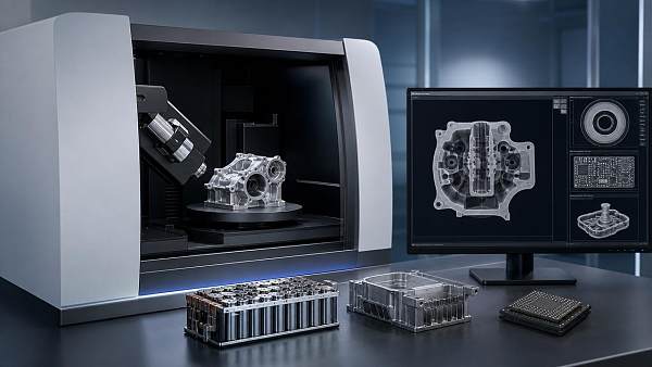
Here, the best measurement strategy is not always the fastest. It is the one that captures voids, delamination risk, warpage evolution, and thermal-stress indicators with documented traceability. The decision focus shifts from output volume to evidence quality.
Core judgment points
- Can non-destructive inspection reveal hidden structural defects early enough?
- Are measurement records audit-ready for customer qualification and field reliability review?
- Do thermal and dimensional datasets align with failure-mode models?
- Is metrology validated against recognized standards and uncertainty protocols?
This is where institutions focused on intelligent measurement, standards benchmarking, and sensory verification provide wider value. The news story is no longer limited to tools. It includes the decision architecture around those tools.
How scenario needs differ in 2026 packaging metrology
This comparison explains why metrology in semiconductor packaging news should be filtered by application. A headline about faster AOI may matter less in power packaging than a report on calibrated X-ray or thermal deformation mapping.
Practical adaptation moves for measurement planning
A useful response to 2026 market shifts starts with measurement architecture, not isolated tool replacement. The following actions create stronger scenario fit and better investment discipline.
- Map each packaging flow by defect risk, not by department boundaries.
- Prioritize metrology steps that directly influence yield or reliability escape rates.
- Require calibration traceability and uncertainty statements during technical comparison.
- Test correlation between optical, dimensional, and electrical datasets before scale-up.
- Review whether software analytics support real-time control, not only historical reporting.
- Use standards-based benchmarking when comparing international suppliers.
These actions align with the wider direction seen in metrology in semiconductor packaging news. The advantage comes from better decision linkage, not from buying the most complex platform by default.
Common misreads and overlooked points in current packaging news
One common mistake is assuming that every AI-enabled inspection system improves process control. Some improve image sorting but do not improve root-cause visibility. Without verified reference data, prediction quality can drift silently.
Another misread is treating all warpage metrics as interchangeable. Measurement method, temperature condition, and package stage can change the result significantly. This issue appears often in metrology in semiconductor packaging news but is still underestimated.
A third oversight concerns standards alignment. Systems may look technically advanced while lacking strong evidence of calibration rigor, uncertainty control, or international compliance mapping. That weakens benchmarking quality and future audit resilience.
Finally, many reviews underestimate data architecture. Measurement value falls when results remain locked inside separate tools. In 2026, the real competitive edge increasingly comes from connected sensory intelligence and decision-ready verification.
What to do next with metrology in semiconductor packaging news
Use metrology in semiconductor packaging news as a scenario filter, not just a trend feed. Match each headline to packaging type, defect risk, evidence requirement, and data integration maturity before making technical judgments.
A structured next step is to build a comparison matrix covering measurement capability, uncertainty, throughput, standards fit, and analytics readiness. This makes vendor screening and internal alignment more objective.
Where advanced packaging decisions affect broader industrial programs, trusted intelligence sources with benchmarking depth become essential. That is especially true when optical sensing, electrical verification, and dimensional metrology must work as one system.
In 2026, the most important signal in metrology in semiconductor packaging news is clear. Measurement is moving from support function to strategic control layer. Those who evaluate by scenario will make stronger quality, sourcing, and investment decisions.
Recommended News
 Jul 04, 2026Advanced Packaging Metrology: Choosing Tools for Warpage and Alignment ControlAdvanced packaging metrology guide for choosing the right tools for warpage and alignment control. Learn how to improve yield, ramp stability, and tool selection with practical insights.
 Jun 30, 20263D Scanning Software Supplier Checklist for Integration and Support3D scanning software supplier checklist for integration and support: learn how to compare technical fit, data traceability, scalability, and service quality for a smarter, lower-risk choice.
 May 28, 2026Semiconductor Packaging Metrology News: Key Shifts in 2026Metrology in semiconductor packaging news for 2026 reveals how AI, traceability, and scenario-based measurement reshape yield, reliability, and smarter investment decisions.
 May 23, 2026Industrial CT Scanner Wholesale for Hidden Defect ChecksIndustrial CT scanner wholesale solutions help quality teams detect hidden defects faster, improve traceability, and compare systems for safer, more consistent inspections.
 May 19, 2026Future of X-Ray CT in Industry: Best Use CasesFuture of X-Ray CT in Industry: discover the best use cases for defect detection, assembly verification, and faster root-cause analysis to reduce risk and improve quality.
 May 15, 2026Industrial CT Scanner Wholesale: Cost, Throughput, and Hidden LimitsIndustrial CT scanner wholesale insights on real cost, throughput, and hidden limits. Learn how to compare systems, avoid costly mistakes, and choose the right fit for production.
 May 12, 2026Future of X-Ray CT in Industry: Speed vs AccuracyFuture of x-ray ct in industry: explore how manufacturers balance speed vs accuracy for reliable inspection, faster decisions, and smarter CT investment planning.
 May 08, 20263D Scanning Mesh Quality Benchmarks Worth Checking Before You Compare Systems3d scanning mesh quality benchmarks matter before you compare scanner speed or price. Learn the key checks for mesh integrity, CAD readiness, and lower procurement risk.
 May 08, 20263D Scanning Speed vs Resolution: What Matters More for Shorter Inspection Cycles?3d scanning speed vs resolution: learn how to shorten inspection cycles by balancing throughput, defect detection, and data quality with smarter, application-based scanning decisions.
 May 07, 2026CT Scanning Resolution Metrics That Matter for Internal Defect AnalysisCT scanning resolution metrics explained for internal defect analysis. Learn how voxel size, contrast, noise, and artifacts affect flaw detection and compare CT systems with confidence.
 May 05, 2026Industrial CT Scanner Wholesale: What Matters Beyond Unit PriceIndustrial CT scanner wholesale buyers should look beyond unit price. Compare TCO, resolution, uptime, software, compliance, and support to secure stronger ROI and lower risk.
 May 04, 2026How to Compare a Semiconductor Metrology Equipment Supplier Without Missing Critical SpecsSemiconductor Metrology Equipment Supplier comparison guide: learn how to verify critical specs, validate real-world performance, and choose a supplier that fits your process, data, and compliance needs.
 Apr 24, 20263D Scanning for Quality Control: Where Errors Begin3D Scanning for quality control starts with setup, calibration, and alignment. Learn how NIST Standards for calibration and advanced metrology solutions improve repeatable inspection.
 Apr 24, 2026Coordinate Measuring Machines or CT Metrology for Hidden Features3D Scanning and Coordinate Measuring Machines vs CT metrology: learn how hidden-feature inspection, industrial sensors, and NIST standards impact accuracy, speed, and smarter QA decisions.