Can Hyperspectral Imaging Detect Defects Standard Cameras Miss?
Time
Click Count
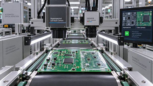
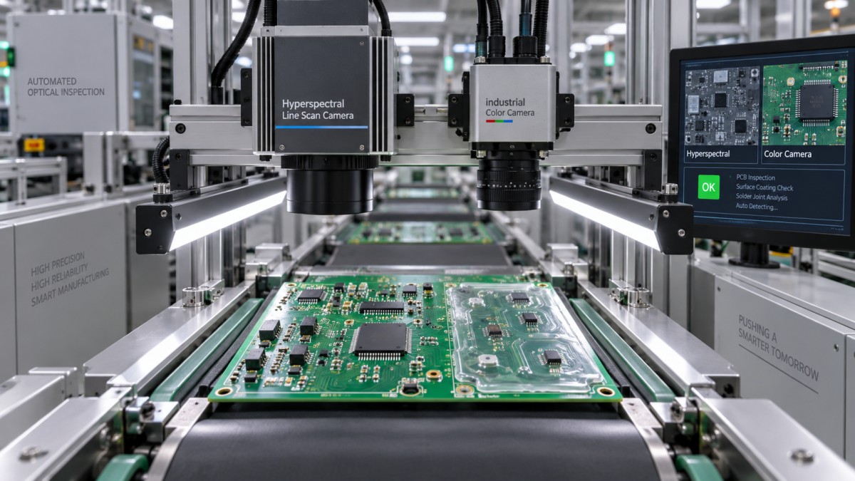
Yes—hyperspectral imaging can detect some defects that standard cameras miss, particularly when the difference is in material composition rather than visible shape or color. On a circuit board, a residue, coating variation, or substituted polymer may look similar to an acceptable surface in an RGB image yet respond differently at selected wavelengths. That extra contrast can support inspection decisions, provided it is strong enough to survive production variation.
It is not a universal upgrade to automated optical inspection. Hyperspectral imaging does not automatically expose buried solder defects, measure electrical performance, or identify trace contamination at reliability-relevant concentrations. Its value depends on a specific question: does the target defect produce a measurable spectral difference that simpler inspection cannot capture reliably?
What a standard camera loses—and hyperspectral imaging preserves
An RGB camera records light through three broad color channels. Different materials can produce similar red, green, and blue values even when their reflectance differs at individual wavelengths. Hyperspectral imaging records many narrow, generally contiguous spectral bands, creating a spectrum for each spatial pixel. Instead of asking only whether a region looks different, the system can assess how that region interacts with light across the measured range.
This distinction matters when acceptable and defective surfaces have similar visible appearances. A clear residue on a solder mask may barely change its apparent color, while producing spectral contrast under suitable illumination. Conversely, a missing component or displaced connector already creates strong spatial contrast. Collecting a spectrum at every pixel may add little to detecting that defect.
The comparison should not be reduced to hyperspectral imaging versus an ordinary color photograph. Industrial machine vision can use monochrome sensors, ultraviolet or infrared illumination, polarization, structured lighting, and multiple viewing angles. These techniques can reveal differences that an RGB image misses without requiring a full hyperspectral data set.
A defensible evaluation therefore compares hyperspectral inspection with the best practical conventional setup—not with a poorly lit camera image.
Which electronics defects offer a credible advantage?
Hyperspectral imaging is most relevant when the inspection problem concerns exposed materials, residues, or surface condition. Even then, detection must be established for the actual material, substrate, and defect level. A strong signature measured from a bulk chemical does not prove that a thin film of that chemical will be detectable on an assembled board.
Residue inspection illustrates both the opportunity and the risk. Detecting a substantial organic deposit is different from determining whether a board carries enough ionic contamination to threaten reliability. A hyperspectral classifier might recognize a visible or optically accessible residue while missing contamination below its detection capability. It should not replace a validated cleanliness test merely because it produces a convincing contamination map.
Coating inspection requires similar discipline. Detecting an uncoated patch, identifying the coating chemistry, estimating thickness, and assessing cure are separate measurement tasks. Each requires its own relationship between optical response and a reference measurement. A system validated for coverage cannot be assumed to verify all four.
The wavelength range matters more than the “hyperspectral” label
Two hyperspectral systems can deliver very different results because they measure different portions of the spectrum. Visible and near-infrared measurements can distinguish color-related and certain material differences. Short-wave infrared measurements provide access to absorption features associated with molecular bonds, including features relevant to some organic materials. That does not mean every electronics residue has a usable signature in every SWIR instrument.
The useful range depends on the target material, the underlying surface, and the illumination. A residue may have a promising absorption feature outside the instrument’s range. It may also have a feature inside that range but too weak to separate from noise at the exposure time available on the line.
Spectral resolution and spatial resolution impose different constraints. Narrower bands can help separate nearby spectral features, but they also divide the available light into smaller portions. Smaller pixels help resolve localized defects, but a defect occupying only part of a pixel produces a mixed signal with the substrate. More bands do not compensate for a contaminant that is too small or too faint to measure.
Reflective metal surfaces add another complication. Their response changes with viewing angle, illumination geometry, and surface roughness. Shadows between tall components can reduce usable signal, while glare can saturate it. Without controlled acquisition, a classifier may learn lighting differences rather than material differences.
A laboratory separation is not yet an inline inspection result
A stationary sample under carefully arranged lighting offers conditions that an operating production line may not reproduce. Inline inspection must accommodate board motion, component height, product changes, vibration, and a fixed cycle time. The meaningful specification is therefore performance at the intended throughput—not the sharpest spectral image obtainable with unlimited exposure.
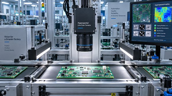
Many hyperspectral systems use line-scan acquisition: the instrument captures a line of spatial pixels and builds an image as the object moves. Reliable results require synchronization between image capture and transport motion. Speed variation, unstable positioning, or registration errors can distort the spectral image or its alignment with conventional inspection data.
Other acquisition architectures have different compromises in spatial sampling, spectral sampling, and capture time. No architecture removes the need to test the smallest relevant defect under the actual acquisition conditions. Data transfer, preprocessing, classification, and communication with the reject mechanism must also fit within the available decision window.
Inspection position can matter as much as sensor choice. A residue may be easier to observe after cleaning but before components or coatings obstruct the surface. An adhesive mix-up may be best checked immediately after dispensing. Moving the inspection upstream can improve optical access, although it may leave later process-generated defects outside its scope.
The system also needs a defined response when measurement quality is insufficient. A shadowed or saturated region should not silently become a passing result. It may require reinspection, a separate station, or an explicit “not assessable” classification.
How to test whether the extra information is actionable
The starting point is a defect definition tied to an acceptance decision. “Detect contamination” is too broad. A useful requirement specifies the substance or residue class, relevant location, smallest actionable deposit or concentration, substrate, and consequence of an escape. Where no acceptable optical threshold exists, the first task is to connect the spectral result to a suitable reference method.
Validation samples should include confirmed defects and representative acceptable variation. Different solder-mask batches, component finishes, permitted flux residues, coating formulations, and supplier materials can all affect spectra. A model trained on one defective batch and one clean batch may distinguish their unrelated manufacturing differences rather than the target defect.
Training and evaluation data should be separated by physical board, batch, or production period where practical. Randomly dividing pixels from the same board between training and testing can create misleadingly strong results because neighboring pixels share material and acquisition conditions.
The decisive measures are defect-level detection, false rejects, unassessable regions, and performance at line speed. Overall classification accuracy is insufficient when defects are rare: a system that passes almost everything can achieve high accuracy while missing the defects that justify its purchase. Results should be reported separately for materially different defect classes and product families.
The baseline test deserves equal attention. Run optimized RGB or monochrome inspection, fluorescence where appropriate, and selected-band imaging against the same samples. If two or three wavelengths provide nearly all the useful discrimination, a multispectral solution may deliver the required result with less data handling and simpler integration.
Hyperspectral imaging can consequently be valuable during development even when it is not the final production sensor. It can help locate useful spectral bands and establish whether material contrast exists. The production decision should follow the validated measurement requirement rather than a preference for the richest data set.
Is hyperspectral imaging worth the cost for electronics inspection?
It can be, when it closes a consequential inspection gap that lower-cost methods cannot close at the required speed and reliability. The strongest case is not “more information per pixel.” It is a demonstrated reduction in a specific class of escapes, false rejects, or destructive testing that exceeds the additional lifecycle cost.
That cost extends beyond the camera. It includes suitable illumination, mechanical integration, shielding from ambient light, computing, calibration references, reference testing, model development, maintenance, and validation after product or process changes. Cleaning optical surfaces and checking instrument stability become part of keeping the inspection decision trustworthy.
A practical economic comparison considers:
- The current cost and frequency of the target defect, including downstream consequences.
- The incremental detection benefit over the strongest feasible alternative.
- The cost of false rejects, manual review, and unnecessary rework.
- Any throughput loss or added handling introduced by acquisition.
- The recurring effort required to keep performance valid across materials and products.
Rare but severe failures deserve separate treatment from routine scrap savings. Their financial consequences may be difficult to estimate, and a short pilot may contain too few genuine defects to demonstrate the required escape rate. Deliberately prepared challenge samples can test detection boundaries, but they should reproduce the relevant production defect rather than an exaggerated version that is easier to identify.
Commercial comparisons should specify usable wavelength range, spatial sampling at the intended field of view, acquisition time, and demonstrated defect performance. A band count or headline frame rate does not establish inspection capability. Access to raw data, calibration procedures, model ownership, and support for material changes also affects whether the installation remains maintainable.
Where the choice becomes clear
Conventional vision remains the stronger starting point when defects are defined by shape, position, visible markings, or surface geometry. Hyperspectral imaging deserves a controlled evaluation when visually similar exposed materials must be separated and their spectral differences can be measured under production conditions. Electrical, X-ray, or other inspection methods remain necessary when the failure mechanism is not optically accessible.
The appropriate deployment may be selective: conventional automated optical inspection for assembly geometry, hyperspectral inspection at a critical material-control step, and reference testing to verify what the spectral classification means. The purchase is justified when that combination changes a reliable acceptance decision—not simply when it reveals differences a standard camera cannot show.
Recommended News
 Oct 16, 2026Can Hyperspectral Imaging Detect Defects Standard Cameras Miss?Is hyperspectral imaging worth the cost for electronics inspection? Discover which defects standard cameras miss, compare alternatives, and learn how to validate ROI before investing.
 Oct 13, 2026Is Hyperspectral Imaging Worth the Cost for Electronics Inspection?How do IEEE standards affect electrical test equipment selection? Compare hyperspectral imaging costs, defect detection, and ROI to make smarter electronics inspection investments.
 Aug 04, 2026How to Evaluate a Hyperspectral Imaging Manufacturer for Calibration and Application FitHyperspectral imaging manufacturer selection starts with calibration integrity, spectral stability, software maturity, and real application fit. Learn what to verify before you buy.
 May 21, 2026Hyperspectral Imaging for Agriculture: Where It Improves Crop DecisionsHyperspectral Imaging for agriculture helps farmers detect stress earlier, optimize inputs, improve crop quality, and make faster, lower-risk field decisions.
 May 21, 20267 Hyperspectral Imaging Applications Worth Tracking in 2026Hyperspectral Imaging applications are reshaping 2026 industries—from semiconductors and food safety to healthcare and defense. Explore 7 high-impact use cases driving smarter inspection and decisions.
 May 21, 2026Hyperspectral Imaging for Mineral Exploration: Faster Ore Mapping or Hype?Hyperspectral Imaging for mineral exploration: discover when it delivers faster ore mapping, clearer alteration targets, and stronger drilling decisions—and when the hype outweighs the evidence.
 May 13, 2026Hyperspectral Imaging for Mineral Exploration in Low-Contrast ZonesHyperspectral Imaging for mineral exploration helps detect subtle ore signatures in low-contrast zones, improving target ranking, reducing risk, and guiding smarter exploration decisions.
 May 03, 2026Hyperspectral Imaging for Mineral Exploration in Early-Stage SurveysHyperspectral Imaging for mineral exploration helps teams rank targets faster, reduce survey risk, and improve early-stage decisions with practical checklists for platform choice, validation, and budget control.
 Apr 24, 2026Hyperspectral Imaging Applications That Moved Beyond LabsHyperspectral Imaging applications now power agriculture, automated vision inspection systems, and 3D Scanning for quality control—see how calibrated, practical solutions improve accuracy and speed.
 Apr 24, 2026What Hyperspectral Imaging Reveals Before Crop Stress ShowsHyperspectral Imaging for agriculture reveals crop stress before visible damage appears, helping teams act earlier with smarter Environmental Monitoring sensors and advanced metrology solutions.
 Apr 24, 2026Hyperspectral Imaging in 2026: Faster Capture, Harder DecisionsHyperspectral Imaging in 2026: compare 3D Scanning, Spectrum Analyzers, Electrical Test, and Industrial Sensors with IEEE Standards and NIST Standards for smarter buying decisions.
 Apr 24, 2026Why Hyperspectral Imaging Misses Defects RGB Cameras CatchHyperspectral Imaging vs RGB: learn why visible defects escape spectral systems on fast lines, and how Industrial Sensors, IEEE Standards, and NIST Standards guide smarter inspection choices.